Hardware Connection
Brief
More information,please reference official documents.DeveloperGuide Orin Nano/NX Core Modules (Orin Nano 4G/8G,Orin NX 8G/16G)fit to carrier board, with 260 pins SO-DIMM connector.
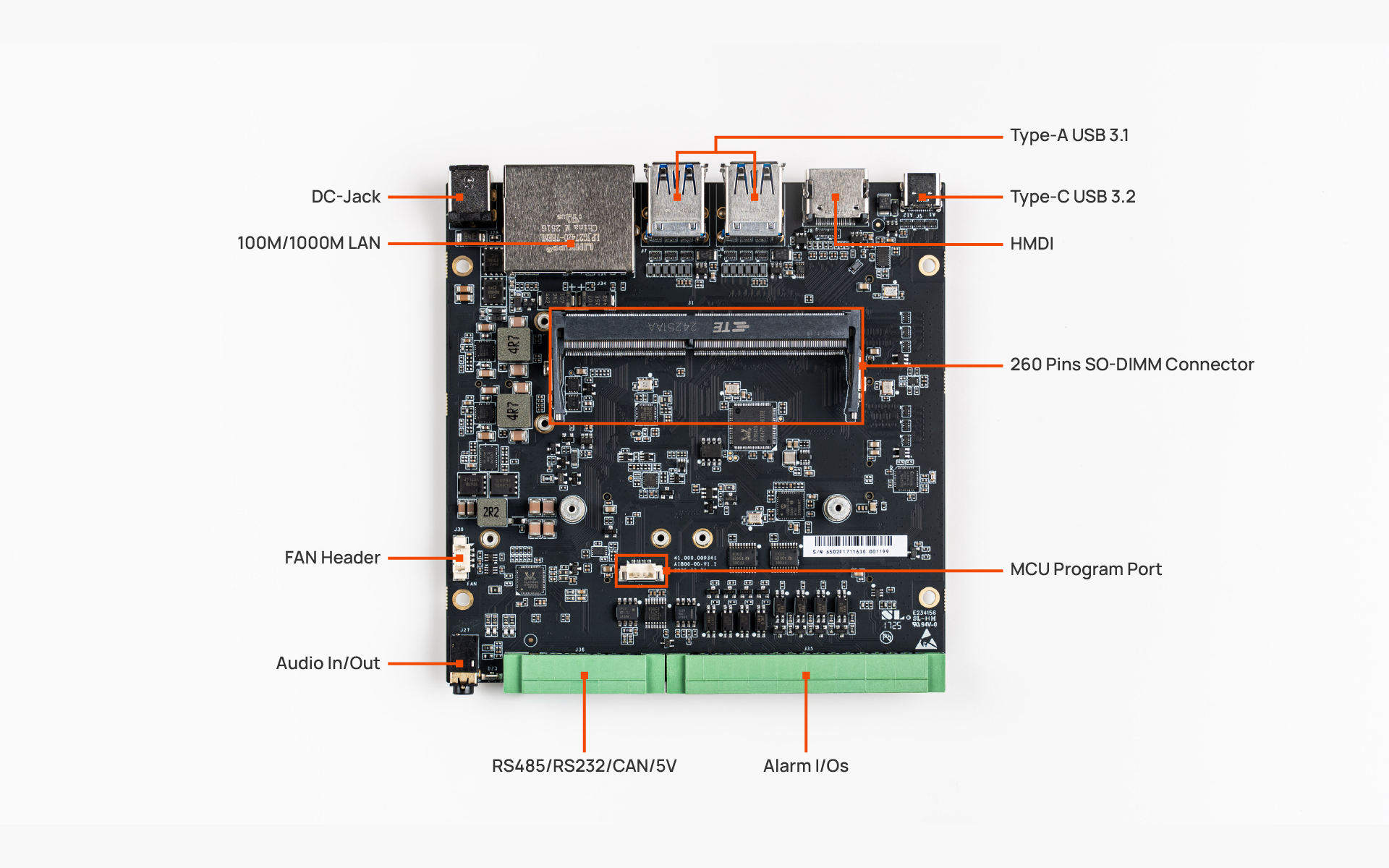
PCBA Interfaces
Top side Interfaces
- DC input from 12 to 36V
- 100M/1000M LAN *2
- USB Type-A *4 support USB3.1
- HDMI (Support: Orin Nano=HDMI 1.4, Orin NX=HDMI 2.1)
- USB Type-C support USB3.2
- SO-DIMM SOCKET 260 pins for Orin Nano/Nx Modules
- PWM FAN Connector
- MCU Program port
- 3.5 Phone Jack for Audio Input and Output
- Terminals for RS485, RS232, CAN, 5V Power Output
- Terminals for DI *4 and DO *4
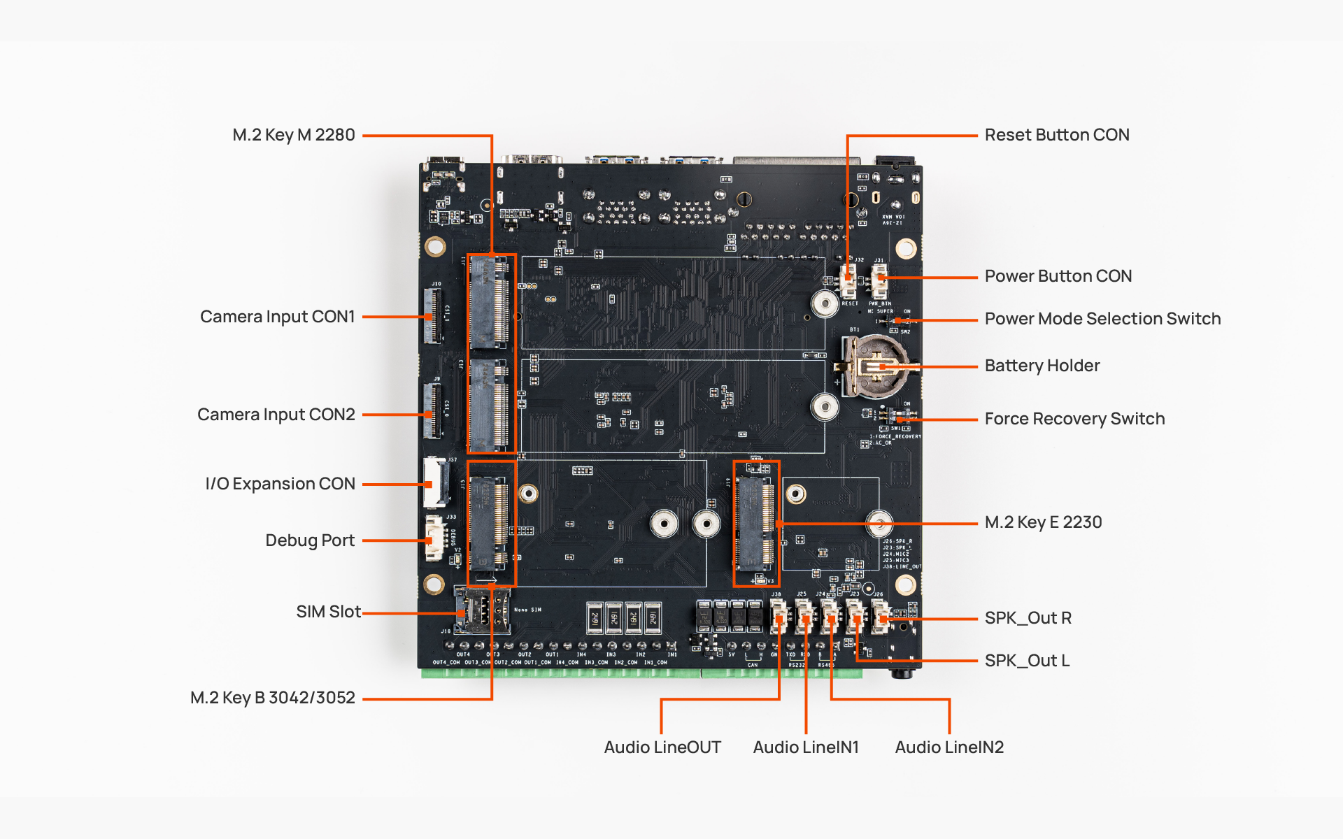
Bottom side Interfaces
- M.2 Key M 2280 for storage, support PCIe *4
- M.2 Key M 2280 for storage, support PCIe *1
- M.2 Key B 3042/3052 for Cellular,support 4G/5G Module
- M.2 Key E 2230 for WiFi&BT
- Camera Input Connector Port1, support 4 Lanes MIPI
- Camera Input Connector Port2, support 4 Lanes MIPI
- I/O Expansion Port, up to 11 GPIOs and 3.3 output
- UART Port for debug
- SIM slot
- Audio Line Output
- Audio Line Input Port1
- Audio Line Input Port2
- Audio Speaker Output L Channel
- Audio Speakper Output R Channel
- Shift switch for power mode selection
- Force Recovery Switch
- Backup Battery Holder
- Power Button Connector
- Reset Button Connector
- Power Mode Selection Switch
Quick connection guide
- Verify all required components in the development kit are complete, including the core module, carrier board, fan, and other peripheral accessories.
- Assemble the fan onto the Orin Nano/NX module:
- Before assembly, confirm thermal grease is applied between the fan and SoC
- Align the fan heatsink with the module, noting the component clearance slots
- Ensure correct orientation of fan bracket and avoid damaging components during tightening
- Confirm the fan is securely locked with bracket and all four screws are tightened
- Insert the fan-equipped Orin Nano/NX module into the 260-pin SO-DIMM socket. After securing the latch, fasten the module to the carrier board using two screws. Finally, connect the fan cable to the PWM FAN connector.
- Install four support standoffs in the mounting holes to elevate the DemoKit. Alternatively, protect the DemoKit using the enclosure kit.
- Flip the carrier board and assemble components on the bottom side:
- Mount RTC Battery CR1220 into BT1 holder (Optional)
- Install SSD in J11 (x4 Lane) or J13 (x1 Lane) M.2 Key M 2280 slot. Recommend system disk in J11, storage expansion in J13 (Optional)
- Install WiFi/BT module in J19 M.2 Key E 2230 slot (Optional)
- Mount 4G/5G module in J15 M.2 Key B 2242/2252 slot, and insert SIM card into J18 slot (Optional)
- Connect Raspberry Pi camera or compatible module to J9/J10 CSI interface (Optional)
- For external buttons: Connect power button to J31 wafer connector, reset button to J32 wafer connector
- For audio functions: Connect external audio source to J25/J24 Line IN, J38 Line OUT to audio devices, J34/J26 Speaker OUT to external speakers, or use J27 3.5mm audio jack
- For additional modules/alarms: Use onboard terminals (RS485, RS232, CAN, DI, DO, 5V power)
- For peripheral expansion: Use J37 FFC connector for GPIO, SPI, I2C, and 3.3V power
- Connect debug serial tool to J33 UART2 interface
- Connect HDMI interface to external display
- Connect wired mouse and keyboard to any two USB Type-A ports
- Insert Ethernet cable into any LAN port
- Connect USB Type-C interface to debug computer
- After verifying all steps, connect power adapter to DC-JACK to begin development and debugging
Software burning and operation reference:System Flashing
Interfaces and instructions
There are related interafces detailed decription,which are using on the Board and product. More information please refer "Jetson Orin NX Series and Jetson Orin Nano Series Pinmux".
NVMe Protocol: Non-Volatile Memory Express, a high-performance, high-concurrency storage protocol designed specifically for SSDs.
PCIe: (Peripheral Component Interconnect Express)is a standard interface for high-speed serial communication, widely used in various expansion cards and devices inside computers. PCIe transmission uses a pair of differential signal lines for data transmission, and each channel contains two pairs of differential signal lines (one for sending and one for receiving). It supports multi-channel configurations, such as x1, x2, x4, x8, etc., indicating the number of channels used. For example, M.2 Key M Port1 supports x4, and M.2 Key M port2 supports x1.
| Feature | Data Rate | Orin Nano | Orin NX |
|---|---|---|---|
| PCIe 3.0 | 1 GB/s @ Lane | Y | Y |
| PCIe 4.0 | 2GB/s @ Lane | X | X |
J11: M.2 Key M (4 Lanes)
This interface supports 4-Lanes PCIe and can be used to connect SSD.
| Pin # | Signal Name | Description | Direction | Pin Type |
|---|---|---|---|---|
| 131 | PCIE0_RX0_N | PCIe 0 Receive 0– (PCIe Ctrl #4 Lane 0) | Input | PCIe PHY |
| 133 | PCIE0_RX0_P | PCIe 0 Receive 0+ (PCIe Ctrl #4 Lane 0) | Input | PCIe PHY |
| 137 | PCIE0_RX1_N | PCIe 0 Receive 1– (PCIe Ctrl #4 Lane 1) | Input | PCIe PHY |
| 139 | PCIE0_RX1_P | PCIe 0 Receive 1+ (PCIe Ctrl #4 Lane 1) | Input | PCIe PHY |
| 149 | PCIE0_RX2_N | PCIe 0 Receive 2– (PCIe Ctrl #4 Lane 2) | Input | PCIe PHY |
| 151 | PCIE0_RX2_P | PCIe 0 Receive 2+ (PCIe Ctrl #4 Lane 2) | Input | PCIe PHY |
| 155 | PCIE0_RX3_N | PCIe 0 Receive 3– (PCIe Ctrl #4 Lane 3) | Input | PCIe PHY |
| 157 | PCIE0_RX3_P | PCIe 0 Receive 3+ (PCIe Ctrl #4 Lane 3) | Input | PCIe PHY |
| 134 | PCIE0_TX0_N | PCIe 0 Transmit 0– (PCIe Ctrl #4 Lane 0) | Output | PCIe PHY |
| 136 | PCIE0_TX0_P | PCIe 0 Transmit 0+ (PCIe Ctrl #4 Lane 0) | Output | PCIe PHY |
| 140 | PCIE0_TX1_N | PCIe 0 Transmit 1– PCIe Ctrl #4 Lane 1) | Output | PCIe PHY |
| 142 | PCIE0_TX1_P | PCIe 0 Transmit 1+ (PCIe Ctrl #4 Lane 1) | Output | PCIe PHY |
| 148 | PCIE0_TX2_N | PCIe 0 Transmit 2– (PCIe Ctrl #4 Lane 2) | Output | PCIe PHY |
| 150 | PCIE0_TX2_P | PCIe 0 Transmit 2+ (PCIe Ctrl #4 Lane 2) | Output | PCIe PHY |
| 154 | PCIE0_TX3_N | PCIe 0 Transmit 3– (PCIe Ctrl #4 Lane 3) | Output | PCIe PHY |
| 156 | PCIE0_TX3_P | PCIe 0 Transmit 3+ (PCIe Ctrl #4 Lane 3) | Output | PCIe PHY |
| 181 | PCIE0_RST* | PCIe 0 Reset (PCIe Ctrl #4) | Bidir | Open Drain 3.3V |
| 180 | PCIE0_CLKREQ* | PCIE 0 Clock Request (PCIe Ctrl #4) | Bidir | Open Drain 3.3V |
| 179 | PCIE_WAKE* | PCIe Wake | Bidir | Open Drain 3.3V |
| 160 | PCIE0_CLK_N | PCIe #0 Reference Clock- | Bidir | PCIe PHY |
| 162 | PCIE0_CLK_P | PCIe #0 Reference Clock+ | Bidir | PCIe PHY |
| 232 | I2C2_SCL | General I2C 2 Clock | Bidir | Open Drain – 1.8V |
| 234 | I2C2_SDA | General I2C 2 Data | Bidir | Open Drain – 1.8V |
J12: M.2 Key M (1 Lanes)
This interface supports 1 Lanes PCIe and can be used to connect SSD.
| Pin # | Signal Name | Description | Direction | Pin Type |
|---|---|---|---|---|
| 40 | PCIE2_RX0_N | PCIe 2 Receive 0– (PCIe Ctrl #7 Lane 0) | Input | PCIe PHY |
| 42 | PCIE2_RX0_P | PCIe 2 Receive 0+ (PCIe Ctrl #7 Lane 0) | Input | PCIe PHY |
| 46 | PCIE2_TX0_N | PCIe 2 Transmit 0– (PCIe Ctrl #7 Lane 0) | Output | PCIe PHY |
| 48 | PCIE2_TX0_P | PCIe 2 Transmit 0+ (PCIe Ctrl #7 Lane 0) | Output | PCIe PHY |
| 52 | PCIE2_CLK_N | PCIe 2 Reference Clock– (PCIe Ctrl #7) | Output | PCIe PHY |
| 54 | PCIE2_CLK_P | PCIe 2 Reference Clock+ (PCIe Ctrl #7) | Output | PCIe PHY |
| 179 | PCIE_WAKE* | PCIe Wake | Bidir | Open Drain 3.3V |
| 219 | PCIE2_RST* | PCIe 2 Reset (PCIe Ctrl #7) | Output | PCIe PHY |
| 221 | PCIE2_CLKREQ* | PCIe 2 Clock Request (PCIe Ctrl #7) | Bidir | PCIe PHY |
| 232 | I2C2_SCL | General I2C 2 Clock | Bidir | Open Drain – 1.8V |
| 234 | I2C2_SDA | General I2C 2 Data | Bidir | Open Drain – 1.8V |
J15: M.2 Key B
This interface is used to connect to the 4G/5G module.
| Pin # | Signal Name | Description | Direction | Pin Type |
|---|---|---|---|---|
| / | USB2_HUB2_P | from usb hub | Bidir | |
| / | USB2_HUB2_N | from usb hub | Bidir | |
| 51 | USBSS2_RX_N | USB SS Receive– (USB 3.2 Ctrl #2) | Input | USB SS PHY |
| 53 | USBSS2_RX_P | USB SS Receive+ (USB 3.2 Ctrl #2) | Input | USB SS PHY |
| 57 | USBSS2_TX_N | USB SS Transmit– (USB 3.2 Ctrl #2) | Output | USB SS PHY |
| 59 | USBSS2_TX_P | USB SS Transmit+ (USB 3.2 Ctrl #2) | Output | USB SS PHY |
| 118 | GPIO01 | WWAN_PWR_ON_N | Input | CMOS – 1.8V |
| 97 | SPI0_CS1* | WWAN_WAKE_EN | Bidir | CMOS – 1.8V |
| 91 | SPI0_SCK | SPI 0 Clock | Bidir | CMOS – 1.8V |
| 89 | SPI0_MOSI | SPI 0 Master Out / Slave In | Bidir | CMOS – 1.8V |
| 93 | SPI0_MISO | SPI 0 Master In / Slave Out | Bidir | CMOS – 1.8V |
| 95 | SPI0_CS0* | SPI 0 Chip Select 0 | Bidir | CMOS – 1.8V |
| 126 | GPIO01 | M2B_RST_N | Input | CMOS – 1.8V |
| / | USIM_RST | Connect to Sim Card for reset | Output | |
| / | USIM_CLK | Connect to Sim Card for clock | Output | |
| / | USIM_DATA | Connect to Sim Card for Data | Bidir | |
| / | USIM_PWR | Connect to Sim Card for power supply | Power | |
| / | USIM_DET | Connect to Sim Card for card detection | Input |
J19: M.2 Key E
This interface is used to connect the WiFi/BT module.
| Pin # | Signal Name | Description | Direction | Pin Type |
|---|---|---|---|---|
| / | USB2_HUB1_P | from usb hub | Bidir | |
| / | USB2_HUB1_N | from usb hub | Bidir | |
| 167 | PCIE1_RX0_N | PCIe 1 Receive 0– (PCIe Ctrl # 1 Lane 0) | Input | PCIe PHY |
| 169 | PCIE1_RX0_P | PCIe 1 Receive 0+ (PCIe Ctrl # 1 Lane 0) | Input | PCIe PHY |
| 172 | PCIE1_TX0_N | PCIe 1 Transmit 0– (PCIe Ctrl # 1 Lane 0) | Output | PCIe PHY |
| 174 | PCIE1_TX0_P | PCIe 1 Transmit 0+ (PCIe Ctrl # 1 Lane 0) | Output | PCIe PHY |
| 173 | PCIE1_CLK_N | PCIe 1 Reference Clock– (PCIe Ctrl #1) | Output | PCIe PHY |
| 175 | PCIE1_CLK_P | PCIe 1 Reference Clock+ (PCIe Ctrl #1) | Output | PCIe PHY |
| 179 | PCIE_WAKE* | PCIe Wake. 47kΩ pull-up to 3.3V on the module. | Bidir | Open Drain 3.3V |
| 182 | PCIE1_CLKREQ* | PCIe 1 Clock Request (PCIe Ctrl # 1). 47kΩ pull-up to 3.3V on the module | Bidir | PCIe PHY |
| 183 | PCIE1_RST* | PCIe 1 Reset (PCIe Ctrl #1). 4.7kΩ pull-up to 3.3V on the module | Output | PCIe PHY |
| 232 | I2C2_SCL | General I2C 2 Clock | Bidir | Open Drain – 1.8V |
| 234 | I2C2_SDA | General I2C 2 Data | Bidir | Open Drain – 1.8V |
| 128 | GPIO05 | Wifi disable control | Output | CMOS – 1.8V |
| 210 | CLK_32K_OUT | M2E_SubClk_32KHz | Output | Clk Soure |
J9: Camera Interface
This interface is CSI0, which supports 4 lanes MIPI and is used to connect to the Camera Module.
| Pin # | Signal Name | Description | Direction | Pin Type |
|---|---|---|---|---|
| 4 | CSI0_D0_N | Camera, CSI 0 Data 0– | Input | MIPI D-PHY |
| 6 | CSI0_D0_P | Camera, CSI 0 Data 0+ | Input | MIPI D-PHY |
| 16 | CSI0_D1_N | Camera, CSI 0 Data 1– | Input | MIPI D-PHY |
| 18 | CSI0_D1_P | Camera, CSI 0 Data 1+ | Input | MIPI D-PHY |
| 10 | CSI0_CLK_N | Camera, CSI 0 Clock– | Input | MIPI D-PHY |
| 12 | CSI0_CLK_P | Camera, CSI 0 Clock+ | Input | MIPI D-PHY |
| 3 | CSI1_D0_N | Camera, CSI 1 Data 0– | Input | MIPI D-PHY |
| 5 | CSI1_D0_P | Camera, CSI 1 Data 0+ | Input | MIPI D-PHY |
| 15 | CSI1_D1_N | Camera, CSI 1 Data 1– | Input | MIPI D-PHY |
| 17 | CSI1_D1_P | Camera, CSI 1 Data 1+ | Input | MIPI D-PHY |
| 114 | CAM0_PWDN | Camera 0 Powerdown or GPIO | Bidir | CMOS – 1.8V |
| 116 | CAM0_MCLK | Camera 0 Reference Clock | Bidir | CMOS – 1.8V |
| 213 | CAM_I2C_SCL | Camera I2C Clock. 2.2kΩ pull-up to 3.3V on the module. | Bidir | Open Drain – 3.3V |
| 215 | CAM_I2C_SDA | Camera I2C Data. 2.2kΩ pull-up to 3.3V on the module. | Bidir | Open Drain – 3.3V |
| 130 | GPIO06 | I2C Channel selection, Low for CSI0 | Output | CMOS – 1.8V |
J10: Camera Interface
This interface is CSI1, which supports 4 lanes MIPI and is used to connect to the Camera Module.
| Pin # | Signal Name | Description | Direction | Pin Type |
|---|---|---|---|---|
| 24 | CSI2_D0_P | Camera, CSI 2 Data 0+ | Input | MIPI D-PHY |
| 34 | CSI2_D1_N | Camera, CSI 2 Data 1– | Input | MIPI D-PHY |
| 36 | CSI2_D1_P | Camera, CSI 2 Data 1+ | Input | MIPI D-PHY |
| 28 | CSI2_CLK_N | Camera, CSI 2 Clock– | Input | MIPI D-PHY |
| 30 | CSI2_CLK_P | Camera, CSI 2 Clock+ | Input | MIPI D-PHY |
| 21 | CSI3_D0_N | Camera, CSI 3 Data 0– | Input | MIPI D-PHY |
| 23 | CSI3_D0_P | Camera, CSI 3 Data 0+ | Input | MIPI D-PHY |
| 33 | CSI3_D1_N | Camera, CSI 3 Data 1– | Input | MIPI D-PHY |
| 35 | CSI3_D1_P | Camera, CSI 3 Data 1+ | Input | MIPI D-PHY |
| 120 | CAM1_PWDN | Camera 1 Powerdown or GPIO | Bidir | CMOS – 1.8V |
| 122 | CAM1_MCLK | Camera 1 Reference Clock | Bidir | CMOS – 1.8V |
| 213 | CAM_I2C_SCL | Camera I2C Clock. 2.2kΩ pull-up to 3.3V on the module. | Bidir | Open Drain – 3.3V |
| 215 | CAM_I2C_SDA | Camera I2C Data. 2.2kΩ pull-up to 3.3V on the module. | Bidir | Open Drain – 3.3V |
| 130 | GPIO06 | I2C Channel selection, High for CSI1 | Output | CMOS – 1.8V |
Audio Interface
| Interfaces | Functions | Descriptions |
|---|---|---|
| J27 | 3.5 Audio Phone Jack | Support Audio Output and Mic Input |
| J24 | Mic Input | Mono Audio Output or Mic Input, Pin1=In/Out,Pin2=GND |
| J25 | Mic Input | Mono Audio IOutput or Mic Input, Pin1=In/Out,Pin2=GND |
| J23 | Speaker Output | Right Channel differential output: Pin1=Positive, Pin2=Negative |
| j26 | Speaker Output | Left Channel differential output: Pin1=Positive, Pin2=Negative |
| J38 | Line Output | L/R Chanel Line Output: Pin1=Left, Pin2=Right |
14 Pins Expansion IOs
This interface can be equipped with an expansion board to connect peripheral devices.
| Pin # | Signal Name | Description | Direction | Pin Type |
|---|---|---|---|---|
| 103 | UART0_RTS* | UART #0 Request to Send | Output | CMOS – 3.3V |
| 105 | UART0_CTS* | UART #0 Clear to Send | Input | CMOS – 3.3V |
| / | GND | GND | GND | GND |
| 106 | SPI1_SCK | SPI 1 Clock | Bidir | CMOS – 3.3V |
| 108 | SPI1_MISO | SPI 1 Master In / Slave Out | Bidir | CMOS – 3.3V |
| 104 | SPI1_MOSI | SPI 1 Master Out / Slave In | Bidir | CMOS – 3.3V |
| 110 | SPI1_CS0* | SPI 1 Chip Select 0 | Bidir | CMOS – 3.3V |
| 112 | SPI1_CS1* | SPI 1 Chip Select 1 | Bidir | CMOS – 3.3V |
| 189 | I2C1_SCL | General I2C 1 Clock. 2.2kΩ pull-up to 3.3V on the module. | Bidir | Open Drain – 3.3V |
| 191 | I2C1_SDA | General I2C 1 Data. 2.2kΩ pull-up to 3.3V on the module. | Bidir | Open Drain – 3.3V |
| 185 | I2C0_SCL | General I2C 0 Clock. 1.5kΩ pull-up to 3.3V on module. | Bidir | Open Drain – 3.3V |
| 187 | I2C0_SDA | General I2C 0 Data. 1.5kΩ pull-up to 3.3V on the module. | Bidir | Open Drain – 3.3V |
| / | GND | GND | / | GND |
| / | 3.3V | Power Supply 3.3V with fuse | Output | 3.3V |
Note:
- I2C0 also connect to Type-C USB control and TPM
- CMOS type IOs have been translate to 3.3V from 1.8V
Rear panel expansion IOs
Please note that the Alarm IOs are dry contact.
| Pin # | Signal Name | Description | Direction | Pin Type |
|---|---|---|---|---|
| 218 | GPIO12 | GPIO=Low/high when IN1=high(Open)/low(Short) | Input | dry contact |
| IN1_COM: COM pin | ||||
| 216 | GPIO11 | IN2: GPIO=Low/high when IN1=high(Open)/low(Short) | Input | dry contact |
| IN2_COM: COM pin | ||||
| 206 | GPIO07 | IN3: GPIO=Low/high when IN1=high(Open)/low(Short) | Input | dry contact |
| IN3_COM: COM pin | ||||
| 228 | GPIO13 | IN4: GPIO=Low/high when IN1=high(Open)/low(Short) | Input | dry contact |
| IN4_COM: COM pin | ||||
| 199 | I2S0_SCLK_1V8 | OUT1: GPIO=Low for short, high for open | Output | dry contact |
| OUT1_COM: COM pin | ||||
| 197 | I2S0_LRCK_1V8 | OUT2: GPIO=Low for short, high for open | Output | dry contact |
| OUT2_COM: COM pin | ||||
| 195 | I2S0_SDIN_1V8 | OUT3: GPIO=Low for shor, high for open. | Output | dry contact |
| OUT3_COM: COM pin | ||||
| 193 | I2S0_SDOUT_1V8 | OUT4: GPIO=Low for short, high for open. | Output | dry contact |
| OUT4_COM: COM pin |
| Pin # | Signal Name | Description | Direction | Pin Type |
|---|---|---|---|---|
| 203 | UART1_TXD | Use for RS_485 | Output | CMOS 1.8V |
| 205 | UART1_RXD | Use for RS_485 | Input | CMOS 1.8V |
| 207 | UART1_RTS* | RS_485 enable pin | Output | CMOS 1.8V |
| 99 | UART0_TXD | Use for uart Ransmit (with 3.3 level shifter) | Output | CMOS – 1.8V |
| 101 | UART0_RXD | Use for uart Receive (with 3.3 level shifter) | Input | CMOS – 1.8V |
| / | GND | GND | GND | GND |
| 145 | CAN_TX | FD CAN Transmit | Output | CMOS – 3.3V |
| 143 | CAN_RX | FD CAN Receive | Input | CMOS – 3.3V |
| / | VCC_5V | VCC_5V | Output | 5V |